• Ultra-low RDS(ON)
• Low Gate Charge
• 100% UIS Tested, 100% Rg Tested
• Pb-free Lead Plating
• Halogen-free and RoHS-compliant
Parameter | Value | Unit |
VDS | 100 | V |
VGS(th) | 3.0 | V |
ID (@ VGS = 10V) (1) | 215 | A |
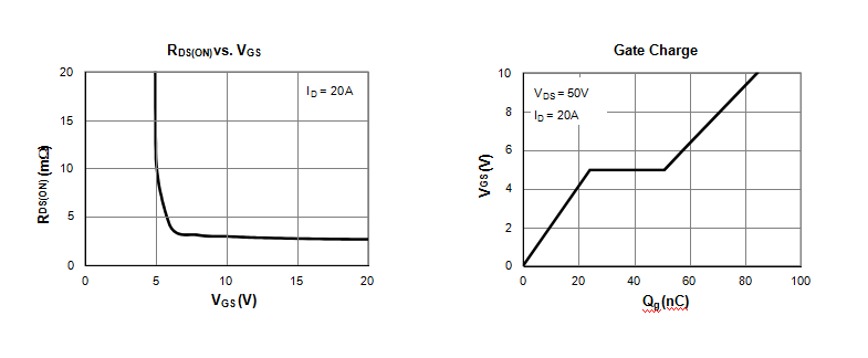
RDS(ON) (@ VGS = 10V) | 3.0 | mW |
Applications
• Motor Driving in Power Tool, E-vehicle, Robotics
• Current Switching in DC/DC & AC/DC (SR) Sub-systems
• Power Management in Telecom., Industrial Automation, CE


Ordering Information
Device | Package | # of Pins | Marking | MSL | TJ (ÀÐC) | Media | Quantity (pcs) |
JMSH1003NC-U | TO-220-3L | 3 | SH1003N | N/A | -55 to 150 | Tube | 50 |
JMSH1003NE-13 | TO-263-3L | 3 | SH1003N | 1 | -55 to 150 | 13-inch Reel | 800 |
Absolute Maximum Ratings (@ TA = 25ÀÐC unless otherwise specified)
Parameter | Symbol | Value | Unit | |
Drain-to-Source Voltage | VDS | 100 | V | |
Gate-to-Source Voltage | VGS | Àâ20 | V | |
Continuous Drain Current (1) | TC = 25ÀÐC | ID | 215 | A |
TC = 100ÀÐC | 136 | |||
Pulsed Drain Current (2) | IDM | 689 | A | |
Avalanche Energy (3) | EAS | 375 | mJ | |
Power Dissipation (4) | TC = 25ÀÐC | PD | 312 | W |
TC = 100ÀÐC | 125 | |||
Junction & Storage Temperature Range | TJ, TSTG | -55 to 150 | ÀÐC | |

Electrical Characteristics (@ TJ = 25ÀÐC unless otherwise specified)
Parameter | Symbol | Conditions | Min. | Typ. | Max. | Unit | |
STATIC PARAMETERS | |||||||
Drain-Source Breakdown Voltage | V(BR)DSS | ID = 250mA, VGS = 0V | 100 | V | |||
Zero Gate Voltage Drain Current | IDSS | VDS = 80V, VGS = 0V | 1.0 | mA | |||
TJ = 55ÀÐC | 5.0 | ||||||
Gate-Body Leakage Current | IGSS | VDS = 0V, VGS = Àâ20V | Àâ100 | nA | |||
Gate Threshold Voltage | VGS(th) | VDS = VGS, ID = 250mA | 2.0 | 3.0 | 4.0 | V | |
Static Drain-Source ON-Resistance | RDS(ON) | VGS = 10V, ID = 20A | TO-263-3L | 3.0 | 3.6 | mW | |
TO-220-3L | 3.2 | 3.8 | mW | ||||
Forward Transconductance | gFS | VDS = 5V, ID = 20A | 58 | S | |||
Diode Forward Voltage | VSD | IS = 1A, VGS = 0V | 0.66 | 1.0 | V | ||
Diode Continuous Current | IS | TC = 25ÀÐC | 215 | A | |||
DYNAMIC PARAMETERS (5) | ||||||
Input Capacitance | Ciss |
VGS = 0V, VDS = 50V, f = 1MHz | 4797 | pF | ||
Output Capacitance | Coss | 900 | pF | |||
Reverse Transfer Capacitance | Crss | 19.1 | pF | |||
Gate Resistance | Rg | VGS = 0V, VDS= 0V, f = 1MHz | 1.9 | W | ||
SWITCHING PARAMETERS (5) | ||||||
Total Gate Charge (@ VGS = 10V) | Qg |
VGS = 0 to 10V VDS = 50V, ID = 20A | 84 | nC | ||
Total Gate Charge (@ VGS = 6.0V) | Qg | 57 | nC | |||
Gate Source Charge | Qgs | 24 | nC | |||
Gate Drain Charge | Qgd | 27 | nC | |||
Turn-On DelayTime | tD(on) |
VGS = 10V, VDS = 50V RL = 2.5W, RGEN = 3W | 21 | ns | ||
Turn-On Rise Time | tr | 35 | ns | |||
Turn-Off DelayTime | tD(off) | 49 | ns | |||
Turn-Off Fall Time | tf | 30 | ns | |||
Body Diode Reverse Recovery Time | trr | IF = 20A, dIF/dt = 100A/ms | 71 | ns | ||
Body Diode Reverse Recovery Charge | Qrr | IF = 20A, dIF/dt = 100A/ms | 127 | nC | ||
Thermal Performance
Parameter | Symbol | Typ. | Max. | Unit |
Thermal Resistance, Junction-to-Ambient | RqJA | 45 | 55 | ÀÐC/W |
Thermal Resistance, Junction-to-Case | RqJC | 0.40 | 0.60 | ÀÐC/W |
Notes:
1. Computed continuous current assumes the condition of TJ_Max while the actual continuous current depends on the thermal & electro-mechanical application board design.
2. This single-pulse measurement was taken under TJ_Max = 150ÀÐC.
3. EAS of 375 mJ is based on starting TJ = 25ÀÐC, L = 0.3mH, IAS = 50A, VGS = 10V, VDD = 50V; 100% test at L = 0.1mH, IAS = 74A. TJ_Max = 150ÀÐC.
4. The power dissipation PD is based on TJ_Max = 150ÀÐC.
5. This value is guaranteed by design hence it is not included in the production test
Changzhou Voha Instrument Co., Ltd.


